+86-755-23289272
sales@bqpwb.com
BQPWB
  • Home
  • Products
    PCBA Board Assembly Industrial Control PCB Assembly Medical PCB Assembly Communication PCB Assembly Automotive PCB Assembly Drone PCB Board HDI PCB Board High Layer PCB High Frequency PCB High Speed PCB 5G Optical Module PCB Semiconductor PCB Thick Copper PCB Industrial Control PCB Consumer Electronics PCB Rigid Flexible PCB RF Antenna PCB
  • About Us
    Company Profile Factory Tour Quality Control Manufacturing Capabilities
  • News
    R&D Updates Industry News
  • Contact Us
  • Language
  • En
    English 中文版
  • PCB/PCBA QUOTE

PCB/PCBA Online Quote

PCS
Gerber & BOM Files

1. Please upload the Gerber & BOM Files and board making instructions

2. The uploaded file format supports ZIP, RAR, 7Z compression package, less than 50MB

1. Please upload the Gerber Files and board making instructions

2. The uploaded file format supports ZIP, RAR, 7Z compression package, less than 50MB

1. Please upload the BOM Files

2. The uploaded file format supports ZIP, RAR, 7Z compression package, less than 50MB

RF Antenna PCB

Discover bqpwb’s RF antenna PCB, engineered for superior performance in radio frequency applications. Our PCBs are designed to enhance signal quality and reliability, offering optimal solutions for RF and antenna technologies.

RF Antenna PCB
  • Home
  • Products
  • RF Antenna PCB

Product center

  • PCBA Board Assembly
  • Industrial Control PCB Assembly
  • Medical PCB Assembly
  • Communication PCB Assembly
  • Automotive PCB Assembly
  • Drone PCB Board
  • HDI PCB Board
  • High Layer PCB
  • High Frequency PCB
  • High Speed PCB
  • 5G Optical Module PCB
  • Semiconductor PCB
  • Thick Copper PCB
  • Industrial Control PCB
  • Consumer Electronics PCB
  • Rigid Flexible PCB
  • RF Antenna PCB
RF Antenna PCB 44

RF Antenna PCB 44

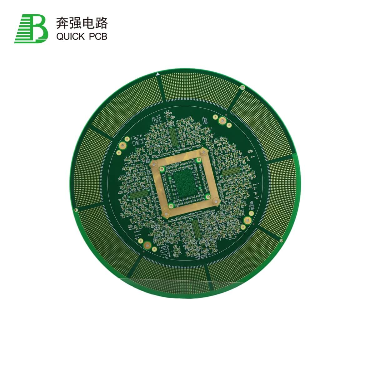
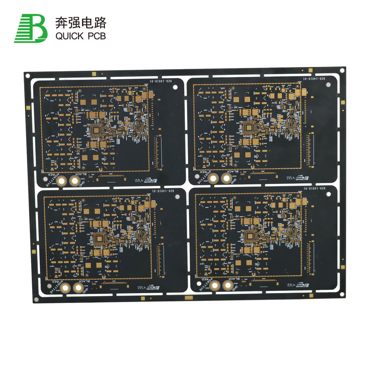
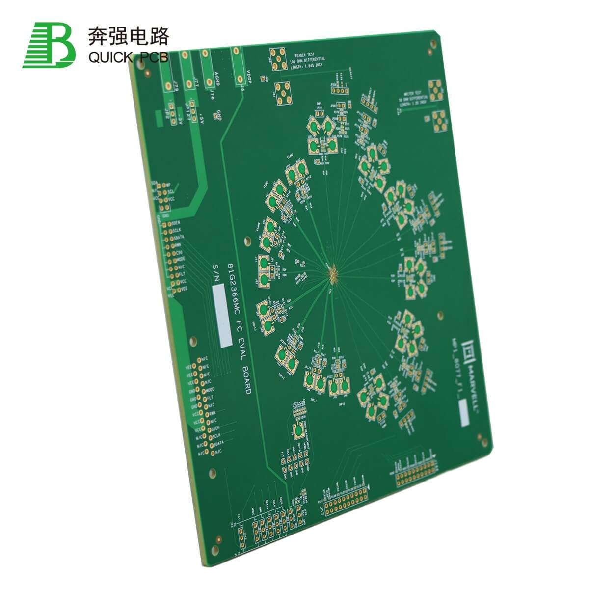
Semiconductor Field Test Probe Card 36 layers 2+N+2 Board Thickness: 4.8 mm Minimum Hole Size: 0.2 mm Hole-to-Line Distance: 0.14 mm

Product Details

RF Antenna PCB 43

RF Antenna PCB 43

Semiconductor Field Test 16 layers 7-step HDI 7+N+7 HDI Thickness: 2.4 mm Minimum hole size: 0.15 mm Hole-to-line distance: 0.07 mm Minimum line width/distance: 0.055/0.055 mm Surface Finish: ENIG

Product Details

RF Antenna PCB 42

RF Antenna PCB 42

Application Characteristic Material Layer Communication High speed+high TG material IT968TC+Shengyi S1000-2M 10L Thickness Min hole diameter Min width/space Internal Number 1.00.1mm Laser hole: 0.10mm, Mechanical hole 0.15mm 100/100um S221021G10 Surface f

Product Details

RF Antenna PCB 41

RF Antenna PCB 41

Application Characteristic Material Layer Communication High speed+high TG material IT968TC+Shengyi S1000-2M 10L Thickness Min hole diameter Min width/space Internal Number 1.00.1mm Laser hole: 0.10mm, Mechanical hole 0.15mm 100/100um S221021G10 Surface f

Product Details

RF Antenna PCB 40

RF Antenna PCB 40

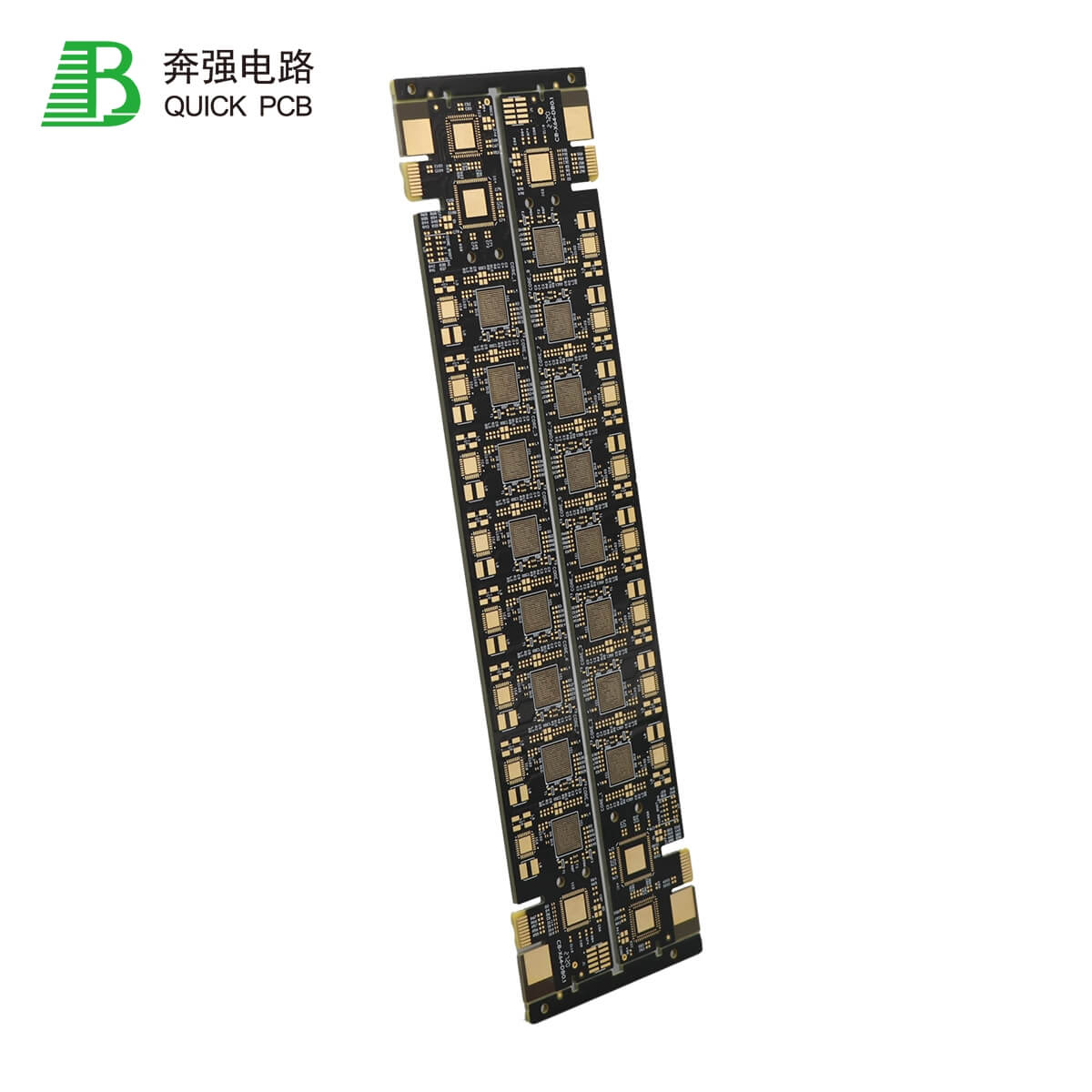
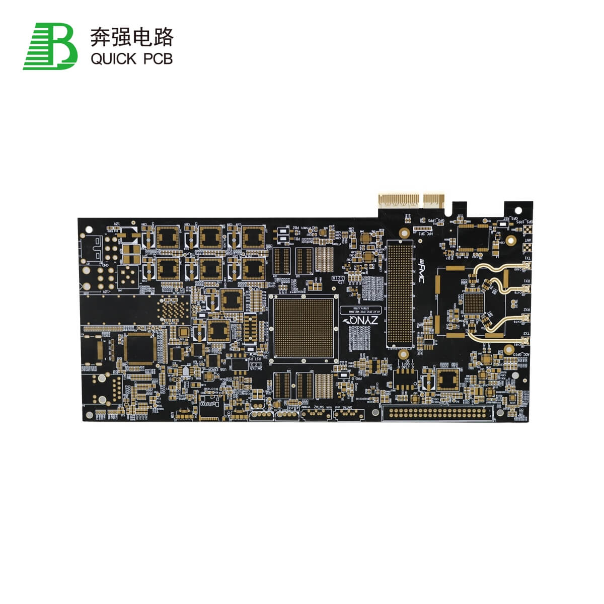
Step golden finger board Material: TU-872SLK 22 layers 1-step HDI 1+N+1 HDI Thickness: 3.0 mm Minimum hole size: 0.25 mm Hole-to-line distance: 0.13 mm Surface Finish: ENIG + Gold finger + Back drill

Product Details

RF Antenna PCB 39

RF Antenna PCB 39

Application Characteristic Material Layer Communication High speed+high TG material IT968TC+Shengyi S1000-2M 10L Thickness Min hole diameter Min width/space Internal Number 1.00.1mm Laser hole: 0.10mm, Mechanical hole 0.15mm 100/100um S221021G10 Surface f

Product Details

RF Antenna PCB 38

RF Antenna PCB 38

Application Characteristic Material Layer Communication High speed+high TG material IT968TC+Shengyi S1000-2M 10L Thickness Min hole diameter Min width/space Internal Number 1.00.1mm Laser hole: 0.10mm, Mechanical hole 0.15mm 100/100um S221021G10 Surface f

Product Details

RF Antenna PCB 37

RF Antenna PCB 37

Application: Computer Product Features: 2x Laser drilling, 3x Pressfit, 2-step HDI board Material: Shengyi S1000-2M Layers: 10L Board Thickness: 1.60.16mm Minimum Hole Size: Laser hole: 0.127mm; Mechanical hole: 0.20mm, Aspect ratio: 8:1 Minimum Line Widt

Product Details

RF Antenna PCB 36

RF Antenna PCB 36

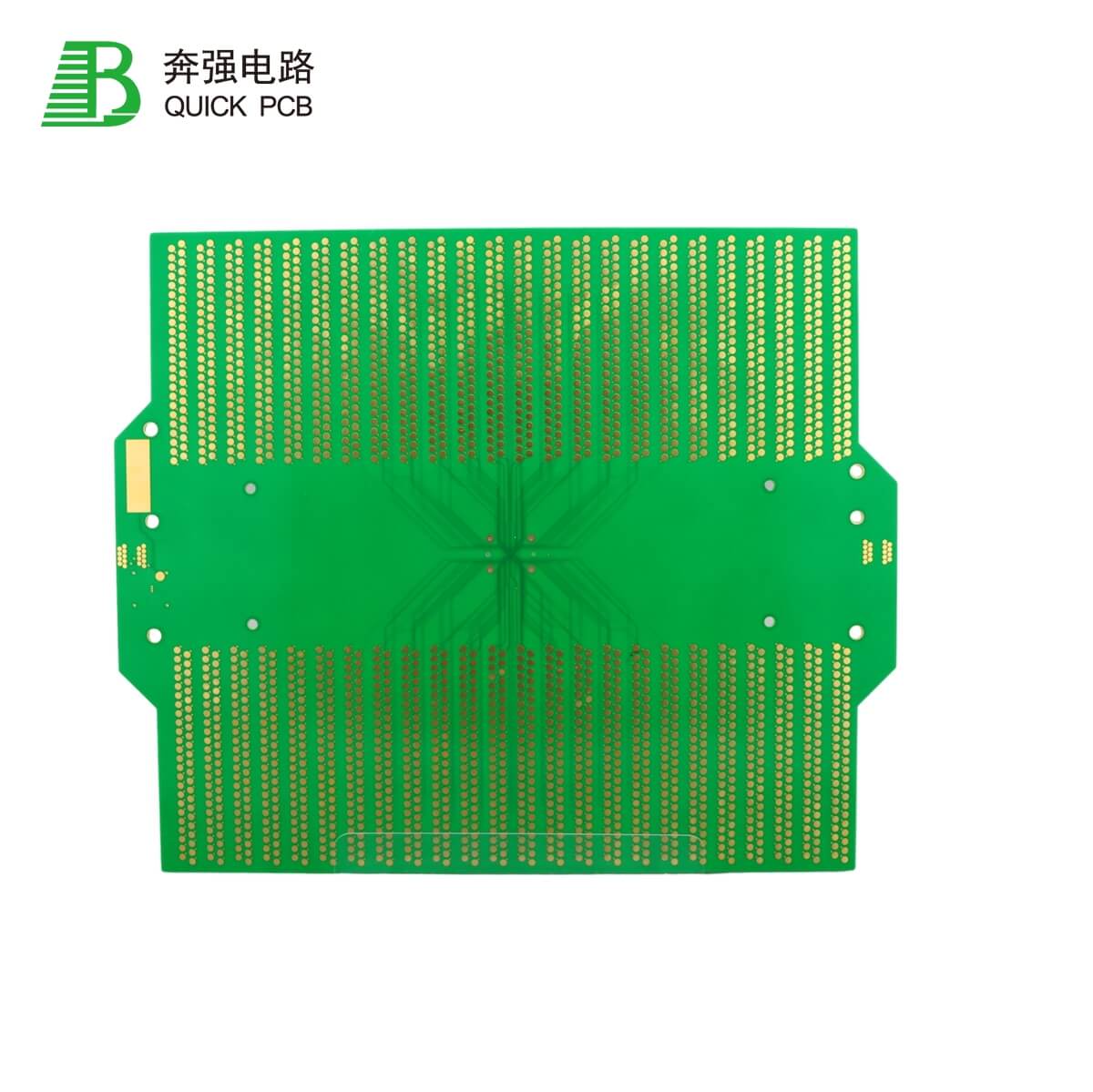
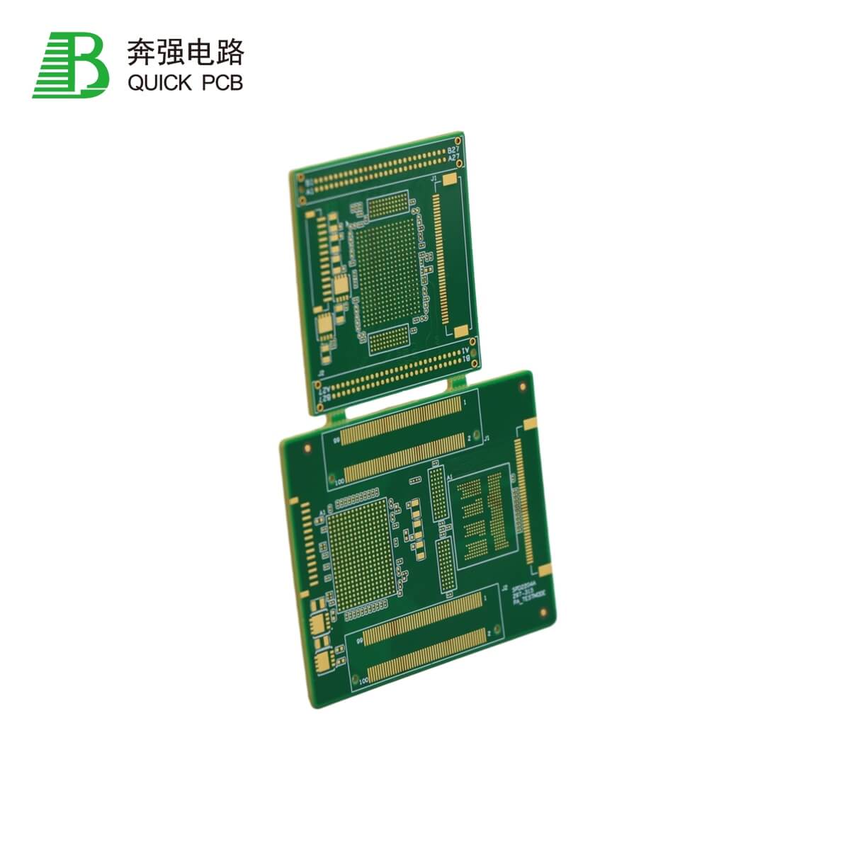
Semiconductor Field Interposer 14 layers 4-step HDI 4+N+4 HDI Thickness: 2.6 mm Minimum hole size: 0.1 mm Hole-to-line distance: 0.1 mm Minimum line width/spacing: 0.06/0.09 mm

Product Details

RF Antenna PCB 35

RF Antenna PCB 35

Fixture Test Board 4 layers Surface Finish: ENIG Minimum Line Width/Spacing: 0.05/0.05 mm Impedance Tolerance: +/-8%

Product Details

RF Antenna PCB 34

RF Antenna PCB 34

Application Characteristic Material Layer Communication High speed+high TG material IT968TC+Shengyi S1000-2M 10L Thickness Min hole diameter Min width/space Internal Number 1.00.1mm Laser hole: 0.10mm, Mechanical hole 0.15mm 100/100um S221021G10 Surface f

Product Details

RF Antenna PCB 33

RF Antenna PCB 33

Application Characteristic Material Layer Communication High speed+high TG material IT968TC+Shengyi S1000-2M 10L Thickness Min hole diameter Min width/space Internal Number 1.00.1mm Laser hole: 0.10mm, Mechanical hole 0.15mm 100/100um S221021G10 Surface f

Product Details

RF Antenna PCB 32

RF Antenna PCB 32

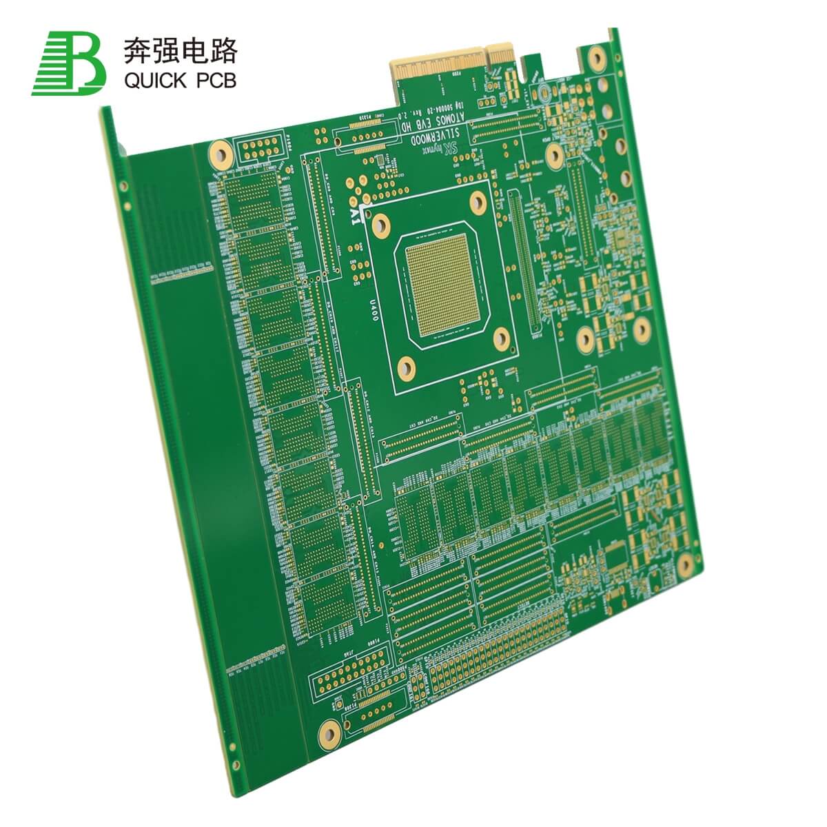
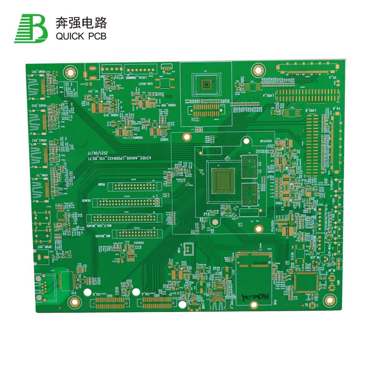
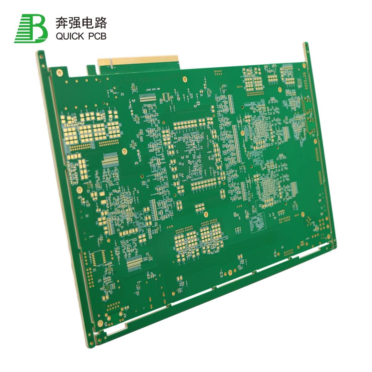
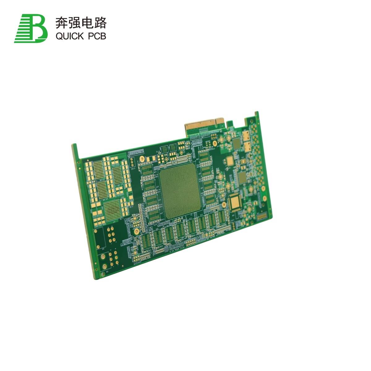
High Speed Chip Server Card Material: TU-872SLK + RO4350 16 layers Board Thickness: 1.6 mm Minimum Line Width/Spacing: 0.075/0.075 mm Surface Finish: ENIG + Gold finger

Product Details

RF Antenna PCB 31

RF Antenna PCB 31

Application Characteristic Material Layer Communication High speed+high TG material IT968TC+Shengyi S1000-2M 10L Thickness Min hole diameter Min width/space Internal Number 1.00.1mm Laser hole: 0.10mm, Mechanical hole 0.15mm 100/100um S221021G10 Surface f

Product Details

RF Antenna PCB 30

RF Antenna PCB 30

Application Characteristic Material Layer Communication High speed+high TG material IT968TC+Shengyi S1000-2M 10L Thickness Min hole diameter Min width/space Internal Number 1.00.1mm Laser hole: 0.10mm, Mechanical hole 0.15mm 100/100um S221021G10 Surface f

Product Details

RF Antenna PCB 29

RF Antenna PCB 29

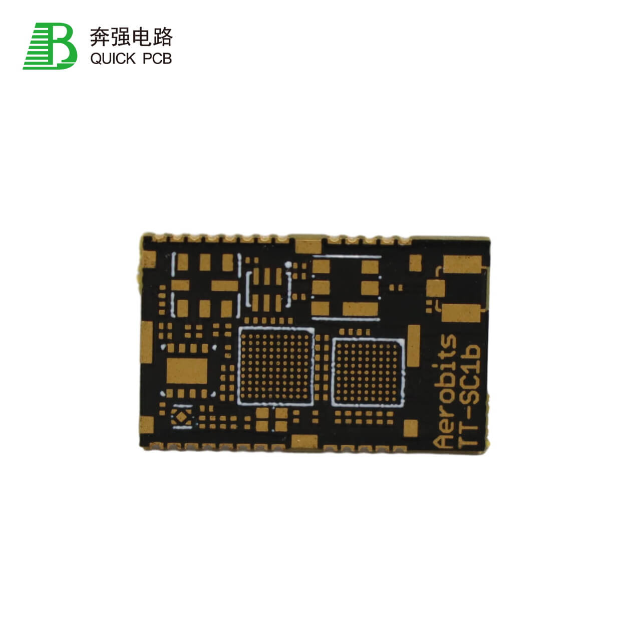
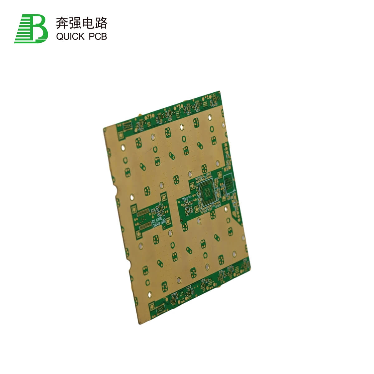
100G Optical Communication Module Material: R-5775G 10 layers 2-step HDI 2+N+2 HDI Surface Finish: Nickel plated palladium

Product Details

  • Previous
  • 1
  • 2
  • 3
  • 4
  • Next
  • 4 Page60 Records
BQPWB

Service Hotline

+86-755-23289272
Email: sales@bqpwb.com

address

Building C5/B6, Yanchuan North Industrial Park, Yanluo Street, Baoan District, Shenzhen, China

ORDER ONLINE

Products

PCBA Board Assembly
Industrial Control PCB Assembly
Medical PCB Assembly
Communication PCB Assembly
Automotive PCB Assembly
Drone PCB Board
HDI PCB Board

About Us

Company Profile
Factory Tour
Quality Control
Manufacturing Capabilities

Quick links

News
Contact Us
Language
Copyright © 2024 BQPWB All Rights Reserved.
map
  • Message
  • E-mail

    sales@bqpwb.com

  • Linkedin

    https://linkedin.com/company/quickpcb

  • WhatsApp

    +86 13760153421